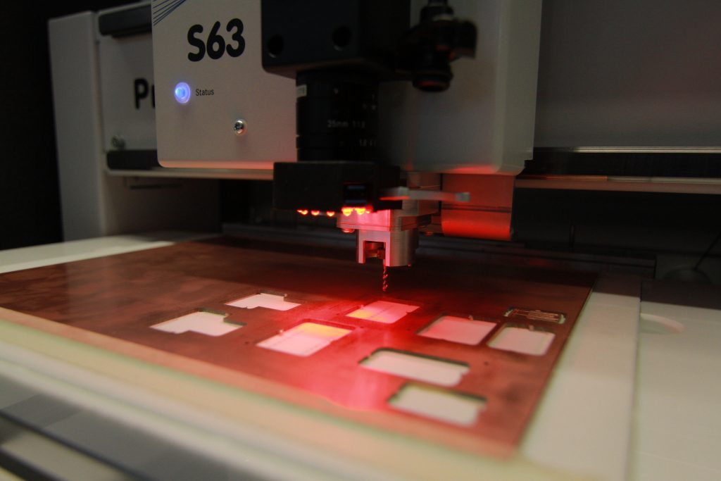
The eLab has a circuit board plotter type LPKF ProtoMat S63 to produce printed circuit boards. A maximum of two-sided PCBs are possible, which should not exceed a size of 20×30 cm. We offer this service to students and chairs for prototyping.
Costs
The costs are calculated from an algorithm based on the main cost factors:
- Base material
- Use of milling tools (distances travelled, milling widths)
- Via rivet count
Design rules
Eagle Designrules can be downloaded below to bypass a preset by hand. The .zip file contains a file with the standardized design rules as well as a file for simplified soldering, which is recommended for non-advanced soldering skills.
The following restrictions can be used for manual input:
Minimum milling width: 0.1mm
Minimum via diameter: 0.4mm
Single and double sided PCBs possible
As format we currently accept only EAGLE *.brd files.
Note for designing
Solder resist is not available, so please make sure that the surfaces to be soldered are sufficiently insulated.
Through-hole plating options
For through-hole plating, LPKF’s EasyContac is available with the following rivet options:
Inner- 0.6 mm, outer diameter 0.8 mm
Inner- 0.8 mm, outer diameter 1.0 mm
inner- 1.0 mm, outer diameter 1.2 mm
inner- 1,2 mm, outer diameter 1,4 mm
Another solution is to put wires through and solder them on both sides. This technique is the best option for a few, single vias.
Steps to reduce milling costs
In principle, it is possible to mill inscriptions into the copper, but this means a lot of milling work and therefore high costs. Therefore we recommend to do without inscriptions.
It is possible to lay a polygon over the entire surface and define it as GND, for example, to save unnecessary milling work. However, this is not necessary, because the LPKF can also be set to electrically isolate everything that is necessary, to mill away only as much as is really necessary, and thus to leave the remaining copper on large open areas. Vias and pads are also automatically milled a little more generously to avoid short circuits. If you still want a polygon as ground plane, the following things should be considered:
The wire-to-wire distance should be set to at least ~0.21mm or 9mil. The main milling work is usually done by a 0.2mm cutter, which at this width goes exactly 2x along each connection and isolates everything efficiently and properly. For values below this (even at exactly 0.2mm), the LPKF uses a 0.1mm cutter instead, which increases costs. At values >0.4mm it moves more than 2x along whereby the costs rise again.
The wire-pad distance should be set higher due to the lack of solder resist. 16mil or 0.4mm has proven to be a good value.
The distance copper/dimension can be set to 0, otherwise a small edge of copper is removed unnecessarily.
Contact
Inquiries about manufacturing or questions about PCB design: